Automatic Optical Inspection is used to check whether the PCB circuit is defective. This work is very important in production, efficient and accurate, and has better performance than traditional LED inspection methods.
1.AOI principle:
Take photo + judge
2.Capture the circuit board image through CCD scanning, use the computer to compare it with the CAM standard graphics and process the logic of the design specification, record the coordinates of the bad points on the circuit board and send the data to VRS for confirmation and repairAOI
Principle picture:
3.The roles and precautions of each post in the AOI process:
AOI
Function: Determine the coordinate position of the dead point on the production board
Note: parameters such as resolution, board edge serial number,
VRS
Function: to judge whether the dead point needs to be repaired and to do simple repair
Note: board serial number, positioning point, offset
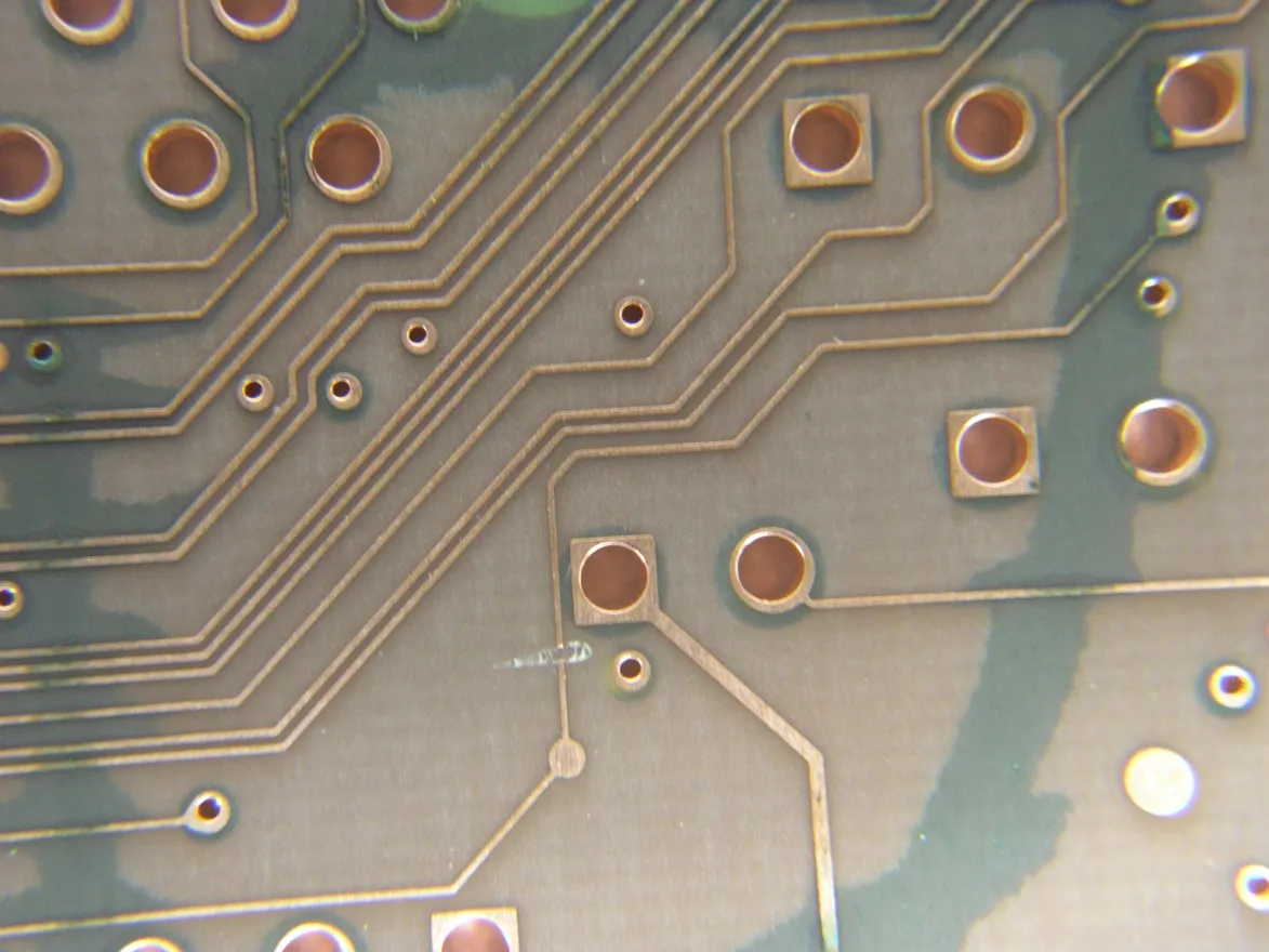
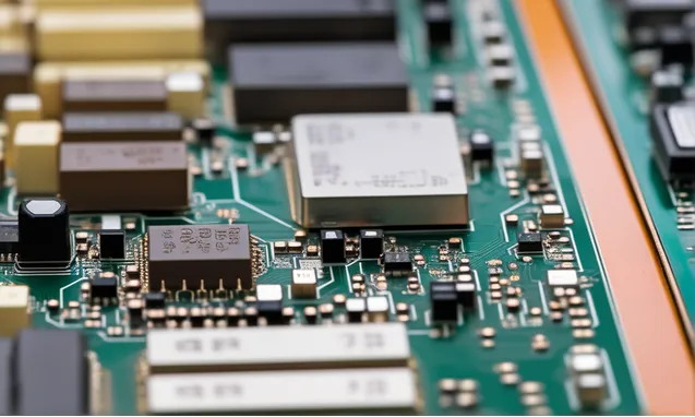
4.Some PCB issue checked by AOI
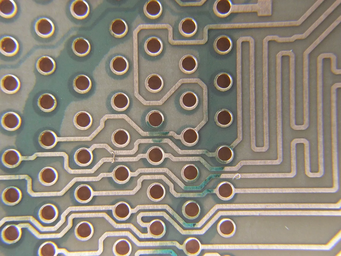
The copper wire on the board surface is a copper wire growing on the copper surface or line surface of the board after etching
The copper wire on the board can cause a short circuit.