
Double-sided PCB
| P/N: Q2P06438A0 | Layer Count: 2L | Min Line W/S: 8/8mil |
| Material: FR-4 Tg 130 | Cu Thickness: 1oz | Min PTH: 0.4mm |
| Board Thickness: 0. 5mm | Surface: ENIG | Application: Automotive |
| Soldermask Color: Green | Board Size: 171.00mmX170.00mm(1-up) | |
| Others: IPC-A-600 Class 3 | ||
Knowledge of double-sided PCBs
Double-sided PCB which both sides are covered with copper and traces and vias can be used to connect the circuits between the two layers to connect the required network. Double-sided PCB can deal with the difficulty of interlaced circuit in single-sided PCB,so it is more suitable to use on more complex circuits than single-sided PCB.
Advantages of double-sided PCBs
Advantages (compared to single-sided boards): convenient,simple wiring,shorter line lengths and so on.
Design operation steps of double-sided PCBs
- Prepare the circuit drawings
- Make a new pcb gerber and load it into the component package
- Programme the circuit
- Place net-list and components
- Automatic layout of components
- Layout adjustment
- Network density analysis
- Set wiring rule
- Automatic routing
- Manual adjustment of routing
Applications of double-sided PCBs
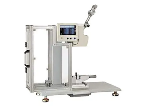
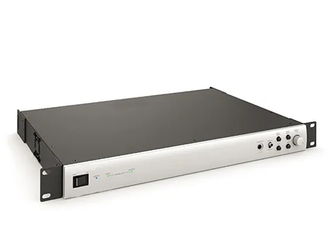
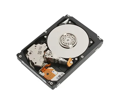
Double-sided PCB can be used widely in various fields and has range of applications:
∗ Hard drives ∗ Car dashboards ∗ Traffic systems
∗ Converters ∗ Vending machines ∗ Amplifiers
∗ UPS power system ∗ Power monitoring ∗ Control relays
∗ Automotive dashboards ∗ Power conversion ∗ Test equipment
Our product display


