
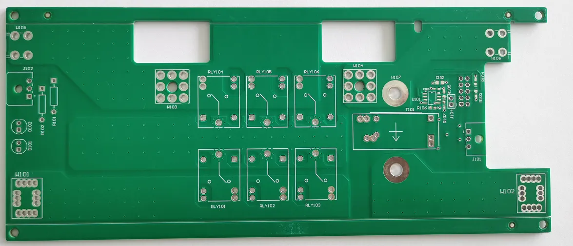
Heavy Copper PCB
| P/N: S4I1 8663A0. | Layer Count: 4L | Min Line W/S: 8/8mil |
| Material:FR-4 Tg 135°C | Cu Thickness: 2/2oz | Min PTH: 0.45mm |
| Board Thickness: 1. 7mm | Surface: ENIG | Application:Industry Control |
| Soldermask Color: Green | Board Size: 273.05mmX158.75mm(1-up) | |
| Others: Impedance Control | ||
Product Features
Advantages of Heavy Copper PCB
Compared to conventional printed circuit boards, a PCB with heavy copper traces offers several advantages.
A Simple & Strong Structure
When integrated into the PCB, high current circuits allow designers to achieve higher density and reduce the layer count. This also maintains the relatively steady but not complex structure of the PCB.Reduce fault status.
Reduces Failure State
Complex printed circuit boards with high current requirements generate more heat. Copper has high heat-conducting abilities and helps to conduct heat away from vital temperature sensitive components.That's why heavy copper is chosen for the board that needs heat dissipation.
Lower Production Costs
Although copper is expensive, rather than use copper cables, using PCBs with heavy copper results in an overall lowering of production costs.The price is relatively cost-effective.
Heavy Copper PCB Manufacturing Capabilities
Victory PCB is a professional pcb manufacturer that can produce high-quality heavy copper PCB products. Check our PCB manufacturing capabilities in the following table.
Fabricating Heavy Copper PCBs

Products application

Some power electronics device require heavy copper PCB to carry larger current and voltage. They are heavy Copper and EXTREME Copper Printed Circuit Boards.
Heavy copper circuit is manufactured with surface copper thickness from 3Oz to 20Oz.
During design the heavy copper pcb, the engineers need to leave enough space between tracks and width to be convenient for production.
Application:
- Power module
- Battery Charger
- medical treatment
- Protection Relays
- welding equipment
- Industrial control
- Automotive electronic components
- high-tech product
- Home appliances
Industry information
Heavy copper is often used in high energy (or high current) printed circuit boards, specifically power electronic equipment and power supply equipment.
Quality Control of Heavy Copper PCB
- Accurately calculate the electroplating area and refer to the influence of the actual production process on the current, correctly determine the required value of the current, grasp the change of the current in the electroplating process, and ensure the stability of the electroplating process parameters;
- Before copper plating, firstly use the debugging board to test the plating solution and make it active;
- Determine the direction of the total current and then determine the order of hanging the boards. In principle, it should be from far to near; Ensure uniformity of current distribution on any surface
- In order to ensure the uniformity of the coating in the hole and the consistency of the coating thickness, in addition to the technical measures of stirring and filtering, pulse current is also required;
- Regularly monitor the current changes during the electroplating process to ensure the reliability and stability of the current value;
- Check if the copper coating thickness of the hole meets the technical requirements
Copper plating process
In the process of heavy copper electroplating, it is necessary to regularly monitor process parameters, often resulting in unnecessary losses due to subjective and objective reasons. In order to do a good job in the heavy copper electroplating process, the following aspects must be achieved
- Add a certain value based on the area value calculated by the computer and the empirical constant accumulated in actual production;
- According to the calculated current value, in order to ensure the integrity of the coating in the hole, a certain value, namely impact current, needs to be added to the original current value, and then restored to the original value in a short period of time
- After 5 minutes of electroplating on the circuit board, remove the substrate and observe whether the copper layer on the surface and inner wall of the hole is intact. It's best that all the holes have a metallic luster.
Welcome to send us RFQs about heavy copper PCB.