PCB Capabilities
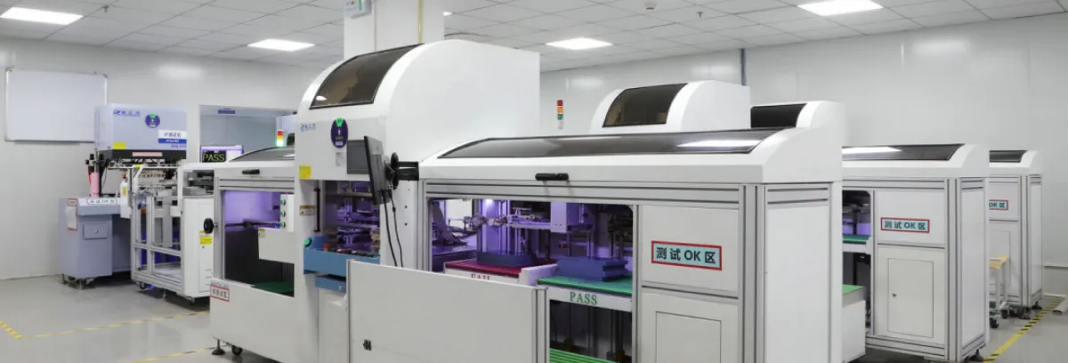
Full range of PCB manufacturing and assembly services to fit all your printed circuit board capability needs.
Victory has introduced world-class PCB production equipment and high-precision testing equipment. We adopted a scientific management model to form a strong and leading process manufacturing capability.
Advanced Manufacturing Equipment
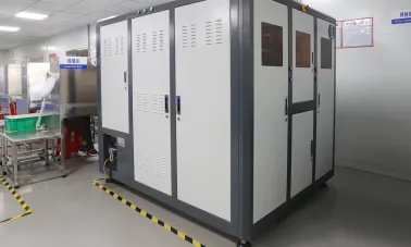
AVI Machine
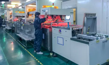
Fully Auto Solder Mask Line
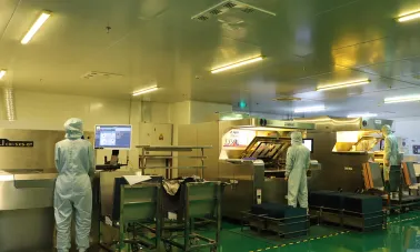
Laser Direct Imaging
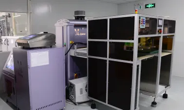
Optima AOI
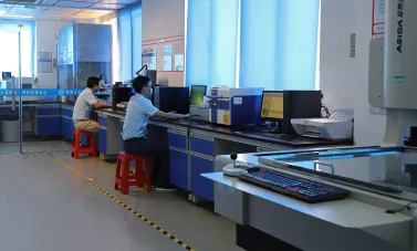
Physical lab
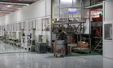
PTH Line
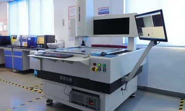
Two-Dimensional Measuring Machine
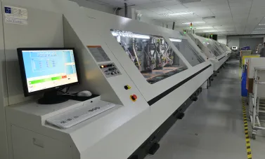
200,000/min speed Drilling Machine
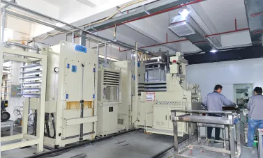
Laminate Equipment
All are available in our processing. Victory can design and process special processes such as controlled depth milling, half hole, mixed pressure and so on.
| Items | Manufacturing Capabilities |
| Material | CEM-3,FR-4(Normal to High Tg), High CTI FR-4, Polyimide(PI), Aluminum Base, Rogers |
| Surface finish | HAL, HASL Leadfree, ENIG,Chem Tin, OSP,Gold Finger, Immersion Silver |
| Min.Core thickness | 2.36mil/0.06mm |
| Prepreg type | 1080, 2116, 7628, 106, 3313, 2165, 1500. |
| Max board size | 22.8X47.2inch/580X1200mm |
| Copper thickness | Min. base copper 1/4Oz |
| Max. base copper 10Oz | |
| Min.board thickness | 2- Layer 0.2mm/8mil |
| 4-Layer 0.35mm/14mil | |
| 6-layer 0.60mm/24mil | |
| 8-Layer 0.8mm/32mil | |
| 10-Layer 1.0mm/40mil | |
| 12-Layer 1.2mm/47mil | |
| 14-Layer 1.4mm/55mil | |
| 16-Layer 1.6mm/63mil | |
| Min.line width/space | 3/3mil inner and outer tracks |
| Min hole size | 4mil/0.1mm |
| PTH wall thickness | ≧25µm |
| Type of Blind and buried vias | II, III, IV, V, VI...... |
| Min. blind/buried vias | 0.1mm/4mil |
| Min.space between vias and tracks | 0.2mm/8mil |
| Min. space between BGA to tracks | 0.076mm/3mil |
| Min. Solder mask bridge | 0.1mm/4mil |
| Min. BGA | 0.2mm |
| Max.board thickness | 6.0mm/236mil |
| Max. aspect ratio | 12:01:00 |
| AOI (Automatic Optical Inspection) | Max.table size: 685X685mm |
| Max.inspect size: 620X620mm | |
| Max. thickness: 3.20mm(126mil) | |
| Min. thickness: 0.06mm(2.36mil)-core | |
| Min. width/gap: 3mil/3mil | |
| Design & Test | 3mil track width, 3mil tracks width/gap, IPC class 2/IPC class 3,Flying probe/tooling test, Differential impedance, TDR testing, Automatic optical inspection |
| Board thickness Tolerance | ±0.10mm(4/6layers) |
| ±0.13mm(8/10layers) | |
| ±0.15mm(12/14/16layers) | |
| PTH dia. Tolerance | ±0.075mm/3mil(Standard), ±0.05mm/2mil(Advanced) |
| NPTH dia. Tolerance | ±0.05mm/2mil(On laminate area) |
| ±0.03mm(On ground area) | |
| Hole location Tolerance | ±0.075(Standard) ±0.05mm(Advanced) |
| ±0.13(2nd drilled hole to 1st drilled hole location (mm)) | |
| Slot size tolerance | ±0.075mm(board thickness≤1.0mm) |
| ±0.10mm(board thickness>1.00mm) | |
| V-CUT Remain thickness tolerance | ±0.10mm(Standard), ±0.076mm(Advanced) |
| Peelable mask Thickness | ≥8mil(0.2mm) |
| Insulation Resistance | >1012Ω |
| Through hole Resistance | <300Ω |
| Current breakdown | 10A |
| Peel Strength | 1.4N/mm |
| S/M Abrasion | >6H |
| Thermal stress | 288℃ 20Sec |
| Test Voltage | 20-300V |
| Impedance control | (50Ω-100Ω)±10%(Standard)、 (50Ω-100Ω)±7%(Advanced) |
PCB Delivery Lead Times
|
Layer
Area
|
1m² | 1m²≤S≤3m² | 3m²≤S≤5m² | Fast |
| 2L | 4day | 6day | 7day | 1day |
| 4L | 6day | 7day | 8day | 2day |
| 8L | 6day | 7day | 9day | 2day |
| 10L | 9day | 10day | 13day | 5day |
