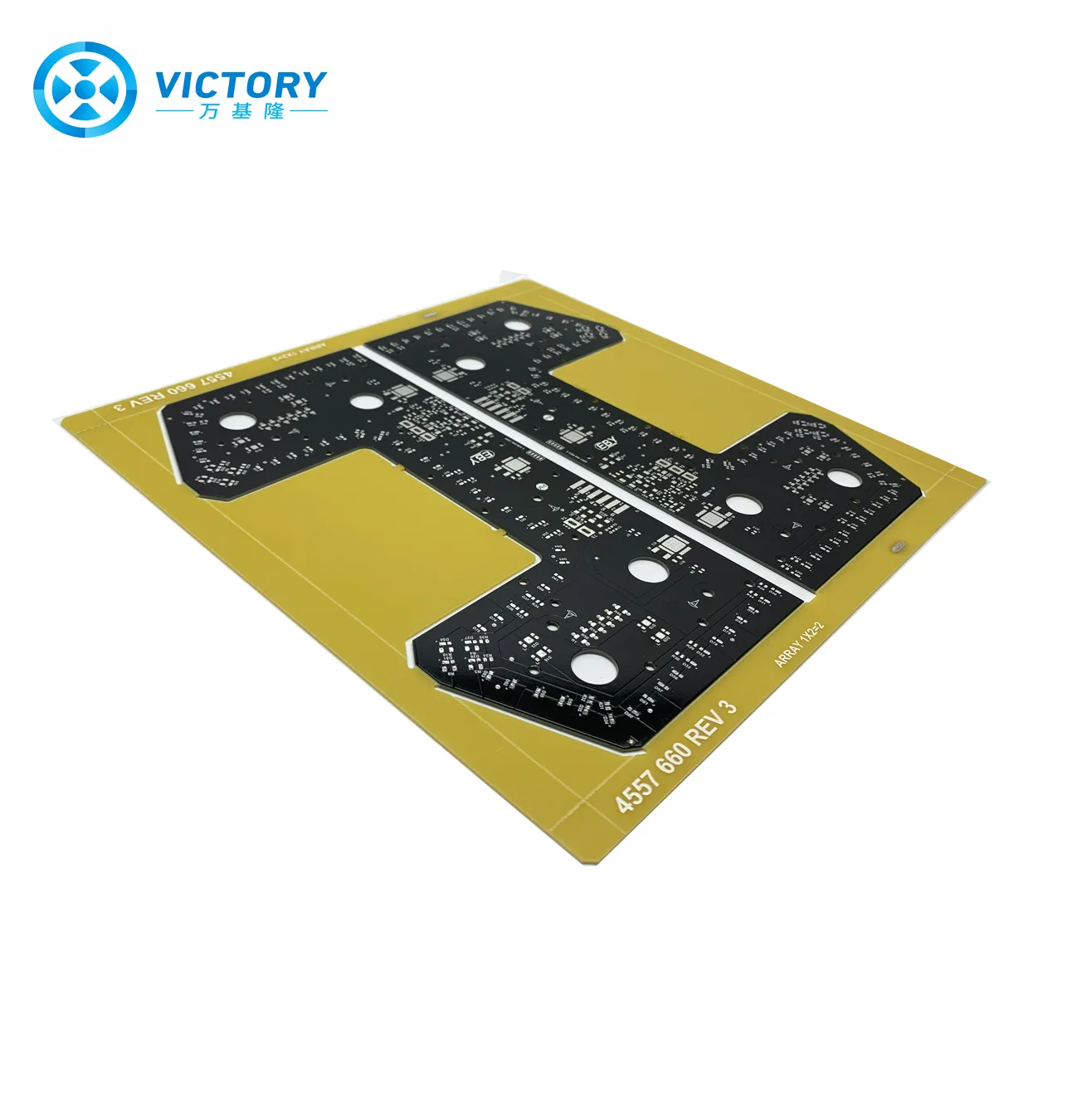
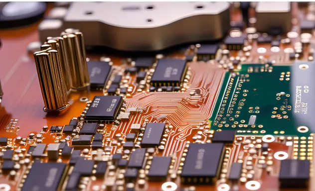
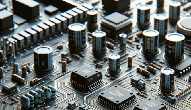
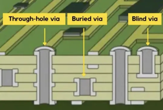
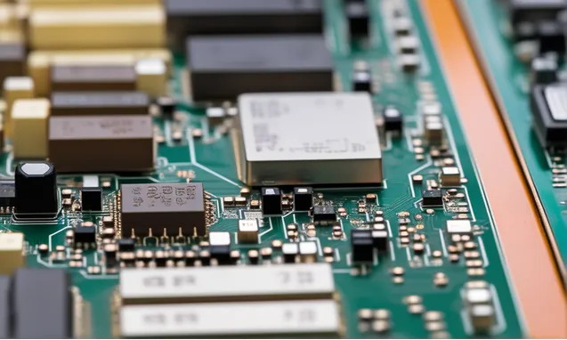
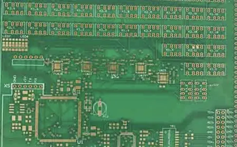
The development of PCB technology has continued until now, and many PCB surface treatment processes have been produced. The common processes are hot air leveling, OSP, electroless nickel plating,immersion Tin/Immersion Au
Hot air leveling
Hot Air leveling, also known as hot air Solder leveling HASL (hot air solder), is a process of coating the PCB surface with molten tin lead solder and leveling with heated compressed air, so that it forms a coating layer that is resistant to copper oxidation and can provide good weldability. Good weldability, hot air is usually solder and copper at the joint of the formation of copper tin gold compounds.
OSP(Organic Solderability Preservative)
Organic coating process OSP is different from other surface treatment processes. It acts as a barrier between copper and air to prevent the surface oxidation of the brazing pad. Organic coating is simple and inexpensive, which makes it widely used in the industry.
Chemical nickel gold (ENIG) electroless Ni plating and electroplating (ENIG) have good weldability. Ni as isolation layer and weldable coating, required thickness ≥3um; Au is the protective layer of Ni, and too much Au dissolved into the solder joint (whether Sn-Pb or Sn-Ag-Cu) will cause “gold brittle”. Therefore, the thickness of Au layer must be limited. The thickness of Au layer used for welding is less than 1? m (ENIG: 0.05 ~ 0.3? m).
Immersion Tin PCB is prone to tin whiskers after immersion process, tin whiskers and tin migration in the welding process will bring reliability problems. After adding organic additives into the leaching solution, the tin layer structure is granular, which overcomes the previous problem, but also has good thermal stability and weldability
isadvantages: The biggest weakness of tin leaching is its short life, especially when stored in high temperature and humidity, Cu/Sn intermetallic compounds will continue to grow until they lose solderability. Therefore, the tin plate can not be stored for too long.
