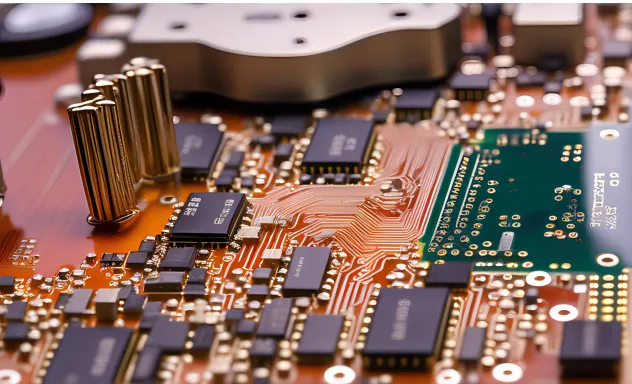
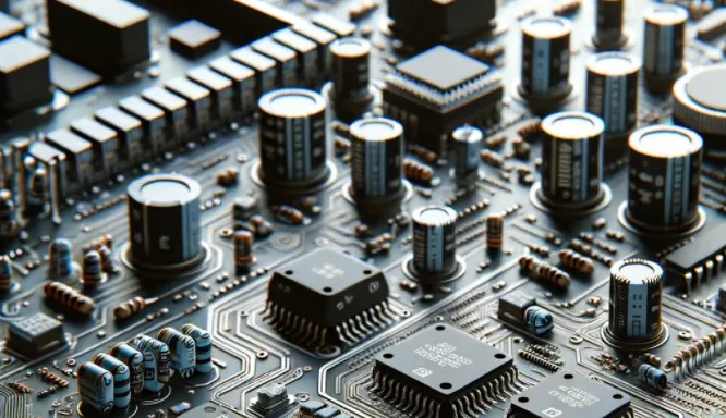
PCB is closely related to our lives,designing the layer stackup for a printed circuit board (PCB) involves many constraints. High-speed designs require careful control of parameters like interplane capacitance, impedance, and crosstalk. Even in slower PCBs, the stackup affects important characteristics like sheet capacitance between planes.
Many stackup considerations can be calculated manually or modeled in circuit design software to simulate a PCB’s impedance. However, altium Designer’s stackup design workflow includes calculating PCB impedance, removing the need for external pcb stackup calculators. Altium’s layer stack manager and routing engine include a field solver to tune impedance across the entire board stackup. This integrated pcb stackup calculator streamlines impedance optimization for high-speed designs.
Calculating Impedance in PCB Stackups
A PCB’s impedance depends on trace geometry, materials, and layer configuration. Accurate impedance calculations require accounting for differences between edge-coupled, embedded, and offset trace topologies. Modeling parameters like copper surface roughness and dielectric dispersion improves results.
IPC-2141 Impedance Formulas
Like many technical fields, PCB stackup design relies on standard equations to calculate parameters. Computing trace impedance requires considering both substrate dielectric properties and the trace shape. Most simple calculators estimate impedance using IPC-2141’s microstrip and stripline equations.
However, IPC-2141 formulas have ±7% accuracy. This makes them unsuitable for high-speed designs with multi-GHz signaling rates. More advanced modeling is needed, but few pcb stackup calculators offer these capabilities.
Modeling Stripline Impedance
The impedance equations show that a stripline’s geometry and substrate impact its impedance. Since dielectric constant appears in the formulas, selecting the right PCB material is critical for achieving target impedance. But surface traces like coplanar waveguides require more than basic calculators.
After choosing a layer stackup, high-speed designers use field solvers to determine the necessary trace dimensions and spacing to attain specific impedance targets.
Altium Designer’s Integrated Impedance Calculator
Altium Designer’s Layer Stack Manager integrates an impedance calculator into the PCB stackup design workflow. The field solver calculates trace impedance based on real-world stackup parameters.
Benefits include:
- Tuning trace impedance by modifying layer stackup
- Refining stackup design to enhance impedance performance
- Accounting for frequency-dependent dielectric effects
- Evaluating tradeoffs between impedance, emissions, and signal integrity
Altium Designer combines the pcb stackup calculator with intelligent autorouting and constraint-driven interface. This facilitates designing impedance-controlled PCB stackups.
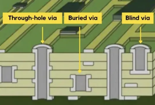
Importance of Layer Spacing and Dielectrics
The spacing between layers (H above) significantly impacts impedance. When developing high-speed PCBs, maintaining stackup integrity is vital for:
- Interplane capacitance for power distribution
- Minimizing loop inductance and crosstalk
- Modeling even/odd mode impedance
The equations also show dielectric constant affects impedance. An accurate pcb stackup calculator must properly model frequency-dependent dielectric constant and loss tangent. This captures their influence on coupling and impedance.
Integrated PCB Impedance Calculators
As PCBs become faster and more complex, their designs require impedance control, crosstalk analysis, and capacitance tuning. Robust impedance modeling is imperative for high-speed performance.
While basic calculators estimate impedance from trace geometry, integration into the design workflow is needed for creating a successful impedance-controlled stackup. Standalone formulas cannot account for all real-world effects.
Altium Designer integrates an advanced pcb stackup calculator into a unified PCB design environment. This enables designers to make informed tradeoffs between impedance, emissions, signal integrity, manufacturability, and other considerations. The end result is a PCB optimized for the target application.
Altium for High-Speed Stackup Design
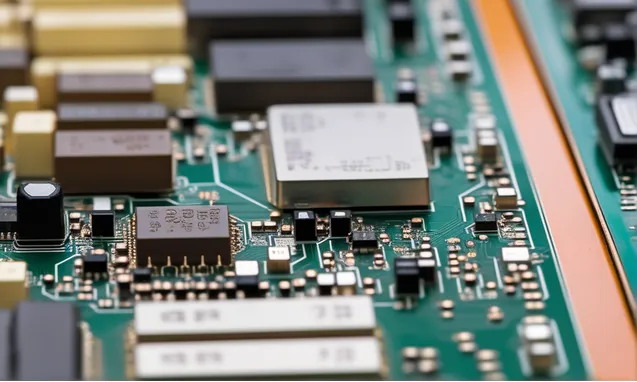
Early PCBs served mainly to interconnect relatively simple components and provide power distribution. As circuits grew more complex, precisely controlling impedance became critical for signal quality. This drove demand for 50-ohm boards.
Modeling PCB Impedance
A trace’s impedance depends on geometry, materials, layering, and other factors. Each trace type – coupled, embedded, or offset – requires specialized modeling for accurate impedance. Basic calculators cannot account for surface roughness or dielectric dispersion, leading to incorrect results.
Altium’s Tunable Stackup Interface
Controlled-impedance designs require integrated power and ground planes. A ground plane provides a low-impedance return path, while power planes distribute clean power. The stackup must carefully balance plane placement and thickness.
Altium Designer tunes the PCB stackup for target impedance and performance. It combines modeling layers, dielectrics, and geometries with intelligent routing and design rule checking. This cohesive workflow enables designing optimized high-speed stackups.
In summary, designing PCB stackups for high-speed or impedance-controlled applications requires advanced modeling tools. Standalone calculators lack the sophistication needed for modern demands. Altium Designer integrates a pcb stackup calculator into a unified PCB design workflow. This enables optimizing stackups by making informed choice between key electrical, mechanical, and manufacturing considerations. The final result is a suitable PCB optimized for its intended application.