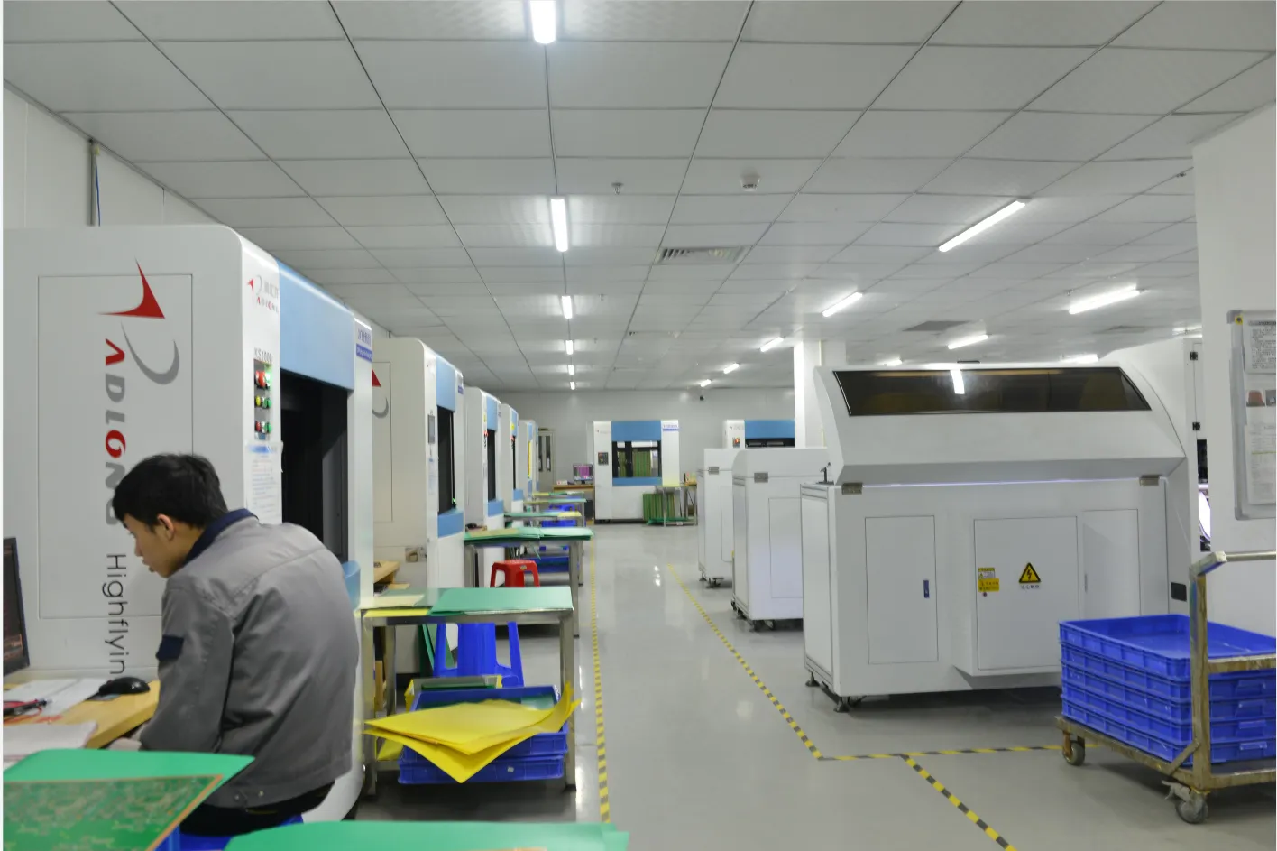
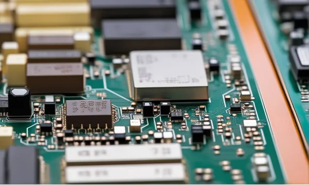
PCB electric testing is the one of the most important process during our PCB manufacturing.
Every PCB must pass electric testing.
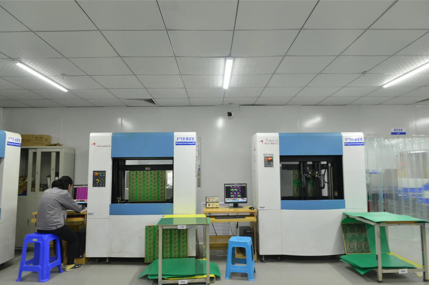
In generally, we have 2 testing methods: Flying probe testing and tooling E-testing, flying probe testing are used for samples and small lots, tooling E-testing are used for middle and mass volume.
1.Flying probe testing:
Flying probe testing is the latest solution to some of the major problems of electrical testing. It replaces the bed of needles with a probe, using multiple motor-driven, fast-moving electrical probes to make contact with the pins of the device and make electrical measurements.
The advantages of using a flying probe test system outweigh the disadvantages. During assembly, for example, such a system provides for production to begin within hours of receipt of the CAD file. As a result, prototype boards can be tested hours after assembly, unlike ICT where costly test development and fixtures can delay the process by days, or even months.
In addition, due to the simplicity and speed of setting, programming and testing, in fact, general technical assemblers, not engineers, can operate and test. Flying probe test also has flexibility to achieve rapid test conversion and rapid feedback of process errors. Also, because flying probe testing requires no fixture development costs, it is a low-cost system that can be placed in front of a typical test process. And because the Flying Probe Tester changes the way to test for low-volume and quick-turnover assemblies, tests that typically take weeks to develop can be obtained in hours.
2.PCB Tooling E-testing
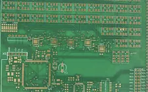
The principle of the PCB test stand is very simple. It connects the pads or test points on the PCB board through metal probes. When the PCB board is powered on, it obtains typical values and phenomena such as the voltage value and current value of the test circuit. Through The data obtained to determine whether the product is qualified.
Composition of PCB test rack
The PCB test frame is customized, which is determined according to the design and production of the PCB board size and the position of the solder joints. It is mainly composed of epoxy board, metal probe, wire and detection interface.
The purpose of PCB test stand
It is mainly used to detect the continuity of the circuit between various points of the PCB board to ensure that the product will not appear unnecessary short circuit and open circuit.