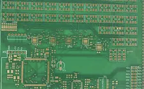
With the development of electronic products in the direction of light, thin and small, PCB is also pushed to high-density and high-difficulty development and the customer’s requirements are getting higher and higher,some customers have designed via in pad in the board. So what is via in pad and how to judge via in pad?
Definition of via in pad
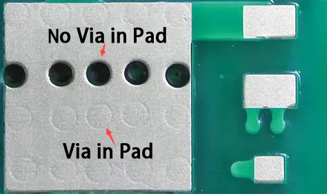
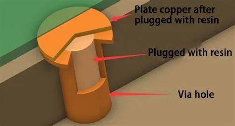
The hole under the pad that is plugged with resin first and then a layer of copper is plated on the inner substrate to make the surface look like a large copper surface and the hole is buried under the pad.
The via in pad can increase the area of the surface pad. For small line width and line spacing, when the pcb wiring and pad area are small, it can reduce the area and the size of the pcb while completing the conductivity.
The via in pad is mainly used in the packaging area of BGA PCB, when the surface needs to be soldered or chip-attached, the requirements for its accuracy and acceptable area are high, and the flatness of the surface is also high, so as to prevent the chip from being uneven which will lead to false soldering or bad joints,we recommend that the conventional surface treatment be ENIG.
How to judge via in pad
- The via in pad required by the customer.
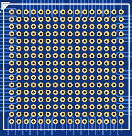
- In the BGA area, the via holes are drilled on the BGA solder joints and the paste layer, the solder mask layer and the opening of the solder mask layer are used to judge.
- The customer requires the hole to be plugged with a certain material (normally below 0.6mm) and capped with copper cap,via in pad is used.
- The BGA area uses the character frame to assist identification.
- The size of the via hole in the BGA area is generally below 0.3mm and the solder joint is generally about 10mil, judged by the size of the D code.
- In the BGA area,should pay attention to the size of the solder mask, paste and opening because the actual size of the solder pad on the circuit layer shall prevail. Don’t be one-sided that it is a via in pad when have the opening touching the hole.
- The opening of BGA solder joints are displayed in a square array and arranged neatly,via holes are punched on BGA solder joints to avoid misjudgment caused by via opening.
- Do not treat PGA as a via in pad in the board by mistake: customers in the PGA area need to insert pin corners. Generally, the area of the pad or the soldering ring is relatively large and the customer’s manual shall prevail.