
HDI PCB 副本
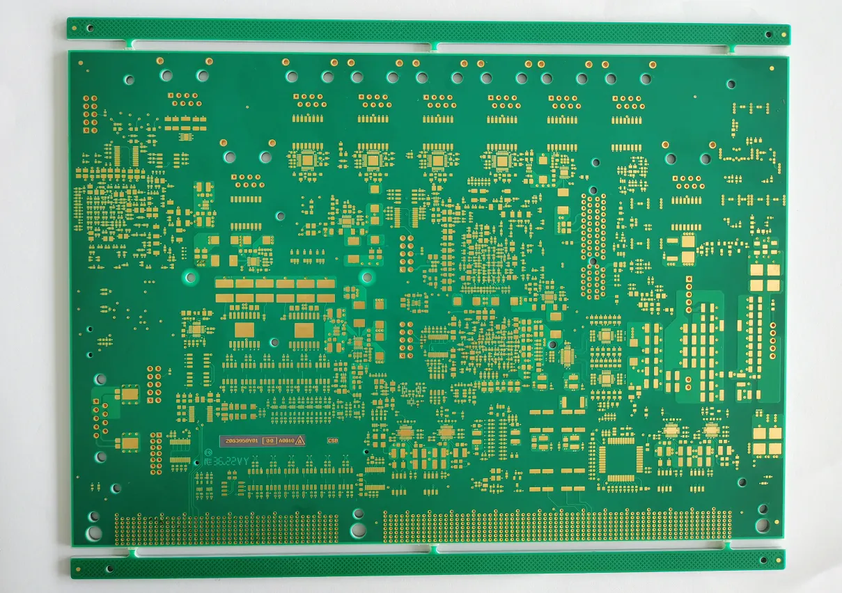
| P/N: S8l1 7966A0 | Layer Count: 8L | Min Line W/S: 4/4mil |
| Material: IT180. | Cu Thickness: 1/0.5oz | Min PTH: 0.1mm |
| Board Thickness: 1. 6mm | Surface: ENIG | Application:Industry Control |
| Soldermask Color: Blue | Board Size: 164.00mmX146. 30mm | |
Product Features
What is HDI PCB
HDI : High Density Interconnection Technology.
Non mechanical drilling, micro blind hole size less than or equal to 150um (6mil), the trace L/S between inner and outer layers less than 4mil, pad diameter ≤ φ The 0.35mm increase layer method for multi-layer board production is called HDI board
Compact design
The combination of micro vias, blind vias, and buried vias greatly reduces board space. With the support of HDI technology, a standard 12-layer through-hole PCB can be simplified into a 6-layer HDI PCB but with the same functions.
Excellent signal integrity
With smaller vias than normal PCBs, all stray capacitance and inductance will be reduced. Combining the technology of bonding vias and vias in pads helps to shorten the length of the signal path. These things that normal vias boards cannot achieve These will lead to faster signal transmission and better signal quality.
High reliability
HDI technology easier wiring and connection, and provides PCBs with better durability and reliability under dangerous environments and extreme conditions.
Save costs
If the traditional pressing process is used and the board layer exceeds 8 layers, then more manufacturing costs are required. But HDI technology can reduce costs and maintain functional purpose.This is one of the reasons why HDI has been promoted.
Products application

HDI is currently widely used in mobile phones, digital (camera) cameras, notebook computers, automotive electronics and other digital products like medical equipment, among which mobile phones are the most widely used. HDI boards are generally manufactured by the build-up method. The more layers are built up, the higher the technical grade of the board. Ordinary HDI boards are basically one-time build-up, and high-end HDI uses two or more build-up technologies, HDI multi-layer circuit board production.
- Mobile Phone
- Digital Products
- Notebook Computers
- Automotive Electronics
- Medical Equipment
Industry information
The development of HDI PCB technology has brought unprecedented design freedom and flexibility to engineers, allowing more components to be placed on both sides of the original PCB as needed, while allowing smaller components to be placed together. This means that HDIPCB ultimately results in faster signal transmission as well as enhanced signal quality.
HDI PCBs are widely used to reduce the weight and overall size of products, as well as enhance the electrical performance of devices.
Most High Density PCB have small tracks width and gap min. 3/3mil, which let engineers realize more functions on one limited dimension PCB.
Shall you have any inquiry about HDI PCB, pls feel free to contact with us.